# USB Clock、Power Control 略
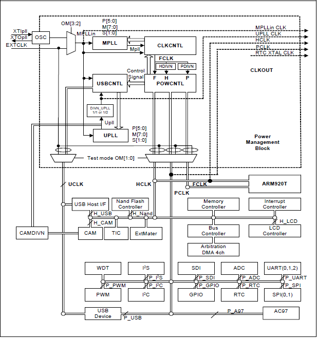
- The main clock source comes from an external crystal (XTIpll) or an external clock (EXTCLK). The clock generator includes an oscillator (Oscillation Amplifier), which is connected to an external crystal, and also has two PLLs (Phase-Locked-Loop), which generate the high frequency clock required in the S3C2440A
- The Clock control logic in S3C2440A can generate the required clock signals including FCLK for CPU, HCLK for the AHB bus peripherals, and PCLK for the APB bus peripherals
- The S3C2440A has two Phase Locked Loops (PLLs): one for FCLK, HCLK, and PCLK, and the other dedicated for USB block (48Mhz)
 |
| Clock Generator Block Diagram |
 |
| ARM920T BLOCK DIAGRAM |
 |
| AHB bus peripherals |
PCLK for the APB bus peripherals(慢)
 |
| APB bus peripherals |
S3C2440採用外部晶振12MHZ,無法滿足CPU工作頻率,因此須利用PLL來提高主頻,S3C2440內部有兩種PLL電路,一種是MPLL,用來產生FCLK、HCLK、PCLK的高頻工作頻率,另一種是UPLL, 用來提供USB裝置的工作頻率。
 |
| Power-On Reset Sequence (when the external clock source is a crystal oscillator) |
within several milliseconds. When nRESET is released after the stabilization of OSC (XTIpll) clock, the PLL starts to operate according to the default PLL configuration. However, PLL is commonly known to be unstable after power-on reset, so Fin is fed directly to FCLK instead of the Mpll (PLL output) before the software newly
configures the PLLCON. Even if the user does not want to change the default value of PLLCON register after reset, the user should write the same value into PLLCON register by software.
The PLL restarts the lockup sequence toward the new frequency only after the software configures the PLL with a new frequency. FCLK can be configured as PLL output (Mpll) immediately after lock time.
從上圖的時序圖中可以看出,當系統上電、復位之後,一開始FCLK跟外部晶振頻率相同,需操作PLL,操作期間,CPU暫時停止工作,直到CPU切換到高頻穩定之後,CPU才開始工作,此段時間稱作 Lock Time。
暫存器操作:
以實作程式碼說明
========================================
1. 先決定FCLK主頻大小
2. 設置MPLL暫存器,使FCLK = 400MHZ,依據手冊公式,
MPLL(FCLK) = (2 * m * Fin)/(p * 2^s)
其中: m = MDIV + 8, p = PDIV + 2, s = SDIV,Fin(輸入頻率) = 12MHz
#define S3C2410_MPLL_200MHZ ((0x5c<<12)|(0x04<<4)|(0x00))
#define S3C2440_MPLL_400MHZ ((0x5c<<12)|(0x01<<4)|(0x01))
 |
| PLL VALUE SELECTION TABLE |
 |
| PLL CONTROL REGISTER |
3. 設置LOCK TIME,設LOCKTIME暫存器
4. 設置HCLK,PCLK大小,設CLKDIVN暫存器
5. 如果HDIV設置為非0,CPU的匯流排模式要進行改變
{
LOCKTIME = 0xffffffff; // default value
CLKDIVN = 0X05 // FCLK:HCLK:FCLK = 1:4:8,CAMDIVN初始值为0,
// 不用再對其設置
/* 如果HDIVN非0,CPU的总线模式应该从“fast bus mode”变为“asynchronous bus mode” */
__asm__(
"mrc p15, 0, r1, c1, c0, 0\n" /* 讀出控制暫存器 */
"orr r1, r1, #0xc0000000\n" /* 設置为“asynchronous bus mode” */
"mcr p15, 0, r1, c1, c0, 0\n" /* 寫入控制暫存器 */
);
/* 判斷是S3C2410還是S3C2440 */
{
/* 現在,FCLK=200MHz,HCLK=100MHz,PCLK=50MHz */
MPLLCON = S3C2410_MPLL_200MHZ;
}
else
{
/* 現在,FCLK=400MHz,HCLK=100MHz,PCLK=50MHz */
MPLLCON = S3C2440_MPLL_400MHZ;
}
}
 |
| LOCKTIME |
 |
| This ratio is determined by HDIVN and PDIVN of CLKDIVN control register |
 |
| CLKDIVN |
參考資料:
- 嵌入式Linux應用開發完全手冊
- S3C2440A 手冊
- http://www.cnblogs.com/zjzsky/p/3560494.html
No comments:
Post a Comment